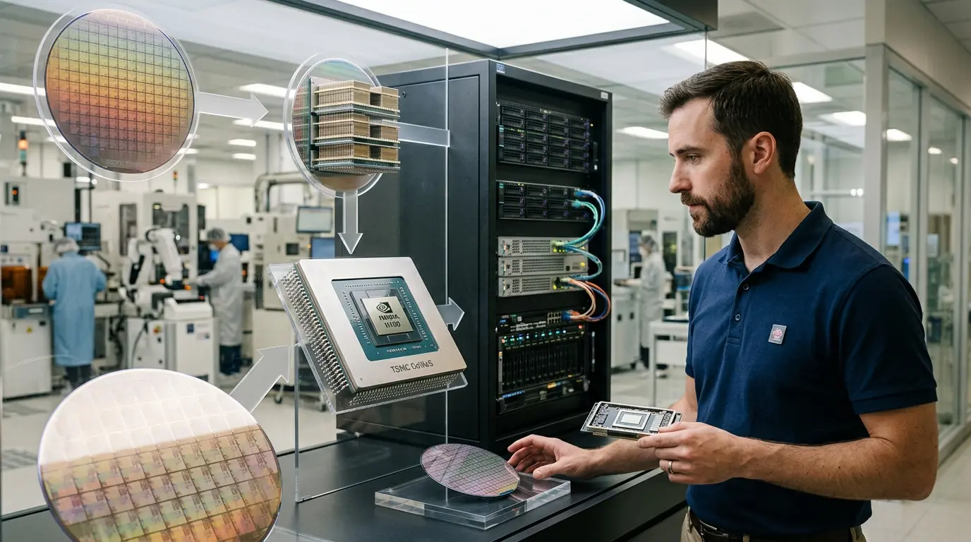
Nvidia designs AI processors and computing platforms, but it does not manufacture most of them in Nvidia-owned semiconductor factories. It uses a fabless business model: Nvidia creates the architecture, chips, boards, systems and software, while outside foundries, memory suppliers, packaging providers and contract manufacturers turn those designs into physical products.
TSMC is the most visible manufacturing partner, but “TSMC makes Nvidia GPUs” is only a partial description. An advanced AI accelerator also needs high-bandwidth memory, substrates, advanced packaging, power components, networking, boards, servers, racks, cooling and final testing. One missing layer can delay the entire system.
For the wider processor, networking, system and software platform, start with our complete Nvidia AI guide. For Nvidia's corporate history and fabless strategy, read what Nvidia does. For the product generations moving through this chain, use the Nvidia AI GPU guide. For the commercial consequences, see how Nvidia makes money from AI. This article owns the physical supply-chain and manufacturing-risk questions.
Nvidia's AI chip supply chain at a glance
| Stage | Main activity | Companies named by Nvidia or central to the stage | Main constraint |
| Architecture and design | Processor, interconnect, board, system and software design | Nvidia and licensed IP/tool providers | Engineering complexity, verification and product cadence |
| Wafer fabrication | Print the semiconductor circuits on silicon wafers | TSMC and Samsung, according to Nvidia's fiscal 2026 10-K | Leading-edge capacity, yield and geographic concentration |
| High-bandwidth memory | Manufacture HBM dies and memory stacks | SK Hynix, Micron and Samsung, according to Nvidia | HBM availability, qualification and packaging alignment |
| Advanced packaging | Combine compute dies, memory and interposer or substrate | Nvidia says it uses CoWoS technology | Packaging capacity, yield, substrate and thermal complexity |
| Board and module production | Build accelerator modules, boards, power delivery and connectors | Contract manufacturers and component suppliers | Component synchronization and quality |
| Assembly, test and packaging | Produce and test final modules, systems and network products | Hon Hai, Wistron and Fabrinet are named by Nvidia | Manufacturing scale, logistics and product transition |
| Networking and systems | Connect GPUs into servers, racks and clusters | Nvidia, OEMs, ODMs, switch and optics partners | Switches, cables, optics, power and liquid cooling |
| Data-centre deployment | Install, power, cool and operate the AI factory | Clouds, enterprises, governments and colocation providers | Electricity, cooling, permits, staff and software readiness |
What “fabless” means
A semiconductor company can design chips without owning a leading-edge fabrication plant. That company is called fabless.
Nvidia controls or heavily influences:
- processor architecture;
- chip and interconnect design;
- accelerator modules and reference boards;
- NVLink, InfiniBand and Ethernet platforms;
- system and rack architecture;
- firmware, drivers, CUDA and libraries;
- product qualification;
- and commercial allocation to customers and partners.
Nvidia generally does not own the full production capacity used to:
- manufacture leading-edge wafers;
- produce HBM stacks;
- perform every packaging step;
- fabricate every board and component;
- assemble every server or rack;
- or build the data centre that operates the equipment.
The fabless model concentrates Nvidia's capital and staff on design and software. It transfers part of the physical production burden to specialized partners, but it does not transfer the supply risk. Nvidia still reserves capacity, makes purchase commitments, qualifies suppliers and coordinates complex product ramps.
The physical product ladder
Supply-chain discussions often use “chip,” “GPU” and “server” as if they were the same object. They are not.
Wafer
A wafer is a circular slice of semiconductor material on which many copies of a chip design are fabricated.
Die
A die is one individual piece cut from the wafer. Advanced processors can combine multiple dies rather than use one monolithic die.
Package
A package combines one or more compute dies with memory and electrical connections. High-end AI accelerators can use advanced interposers and multi-die packaging.
Accelerator module or board
The packaged processor and HBM are placed on a module or board with power delivery, controllers and high-speed links. Examples include PCIe cards and OAM-style modules.
Server
A server combines several accelerator modules with CPUs, memory, storage, network adapters, power supplies, cooling and a chassis.
Rack-scale system
A rack can integrate dozens of accelerators, CPUs, NVLink switches, network switches, power shelves and liquid cooling into one logical system.
Cluster or AI factory
Multiple racks connect through scale-out networking and shared storage, then run through orchestration, scheduling and AI software.
A bottleneck at any level can prevent the final system from shipping or reaching its advertised performance.
Stage 1: Nvidia designs the platform
The supply chain begins years before a wafer enters a foundry.
Nvidia's engineering work includes:
- selecting the workload and performance target;
- defining the processor architecture;
- designing compute, memory and interconnect blocks;
- creating chiplets or multi-die layouts;
- verifying functional correctness;
- designing the package and board;
- co-designing power and cooling;
- developing compilers, drivers and libraries;
- and validating the complete system.
The company also uses licensed intellectual property and electronic-design-automation tools from specialized suppliers. Those tools help engineers describe, simulate, verify and prepare designs for manufacturing. They are an important upstream dependency, but they should not be confused with the foundry that fabricates the wafer.
Why software begins before manufacturing
CUDA, communication libraries and model runtimes must support a new architecture when customers receive it. Hardware without stable software creates unusable inventory. Nvidia therefore develops silicon and software in parallel and gives selected partners early access for qualification.
The complete Nvidia AI guide explains how these hardware and software layers fit together.
Stage 2: TSMC and Samsung fabricate wafers
Nvidia's fiscal 2026 Form 10-K states that it uses foundries including Taiwan Semiconductor Manufacturing Company, or TSMC, and Samsung Electronics to produce semiconductor wafers.
The foundry receives a manufacturing-ready design and uses an extremely complex sequence of deposition, lithography, etching, ion implantation, cleaning and inspection to form transistors and interconnect layers on a wafer.
TSMC's role
TSMC is the dominant manufacturing partner associated with Nvidia's current high-end AI platforms. It supplies leading process technology and advanced packaging capacity at enormous scale.
TSMC does not design CUDA, Nvidia's GPU architecture or the finished DGX system. Its role is to manufacture and package the silicon according to the agreed process and design rules.
Samsung's role
Nvidia also names Samsung as a foundry. Supplier diversification can create resilience, product flexibility and negotiating capacity. A chip design is not automatically portable between foundries: process rules, libraries, physical design and qualification can require substantial work.
Why foundry capacity is scarce
Leading-edge capacity is difficult to expand because:
- a semiconductor fab costs billions of dollars;
- construction and qualification take years;
- specialized tools have long lead times;
- each process requires high yield and precise control;
- and many customers compete for the same nodes.
Nvidia must reserve capacity before final demand is perfectly known. Too little capacity limits revenue; too much can leave purchase commitments and inventory exposed if demand or regulation changes. AI World Today's report on the TSMC capacity crunch and renewed interest in Intel provides a time-bound example of how those constraints can reshape sourcing discussions.
Where ASML fits
ASML makes advanced lithography equipment used by leading semiconductor manufacturers. It is a critical upstream enabler of modern chip production.
ASML is not normally the company that receives an Nvidia design and delivers finished Nvidia GPUs. It sells lithography systems and support to foundries and chip manufacturers. The direct manufacturing relationship for an Nvidia wafer is with the foundry, such as TSMC or Samsung.
The distinction matters:
- Nvidia designs the product;
- a foundry fabricates the wafer;
- ASML supplies essential equipment used inside advanced fabs;
- memory suppliers make HBM;
- packaging and manufacturing partners assemble the complete product.
Calling every company in that chain “Nvidia's chipmaker” removes the actual dependencies.
Stage 3: HBM suppliers make the memory
Modern AI accelerators require enormous memory bandwidth. Ordinary server memory is too far from the processor and too slow for many accelerator workloads.
High-bandwidth memory stacks multiple memory dies vertically and places them close to the processor through an advanced package. It can provide much greater bandwidth and energy efficiency per bit moved than conventional off-package memory.
Nvidia's 10-K says it purchases memory from:
- SK Hynix;
- Micron Technology;
- Samsung.
Why HBM is a separate bottleneck
A foundry can produce the compute die while the final accelerator remains unavailable because the required HBM has not been delivered or qualified.
HBM supply depends on:
- memory-wafer capacity;
- stacking and through-silicon-via processes;
- yield across multiple dies;
- thermal and electrical qualification;
- the exact HBM generation;
- and alignment with advanced packaging capacity.
The compute die, HBM and package must arrive in the correct combination. A surplus of one component does not compensate for a shortage of another.
Capacity is not interchangeable overnight
A product designed for a specific HBM stack cannot automatically accept any available memory. Suppliers must meet electrical, thermal, reliability and performance requirements. Qualification and package design create lead time.
Stage 4: CoWoS and advanced packaging
Nvidia says it uses CoWoS technology for semiconductor packaging. CoWoS is a TSMC advanced-packaging family whose name refers to chip-on-wafer-on-substrate approaches.
At a high level, advanced packaging can:
- place compute dies and HBM close together;
- connect them through a high-density interposer or related structure;
- provide enormous data bandwidth;
- support multiple dies in one package;
- and route power and signals to the substrate and board.
Why packaging became strategically important
Traditional packaging was often treated as a final step after the “real” chip was made. AI accelerators changed that view.
Package design now determines:
- memory bandwidth;
- how many dies can work together;
- power delivery;
- thermal behavior;
- signal integrity;
- yield of the assembled product;
- and ultimately how many finished accelerators can ship.
A wafer-fabrication expansion does not solve a packaging bottleneck by itself.
Packaging yield is multiplicative
A package can contain several expensive components. If one compute die, memory stack, interposer connection or assembly step fails, the economic loss is larger than for a simple low-cost chip.
Manufacturers use testing and known-good-die strategies to reduce that risk, but complexity remains. This is one reason product ramps can be expensive and uneven.
Stage 5: substrates, boards, power and components
The packaged accelerator must be integrated into a working module or board.
That requires:
- package substrates;
- printed circuit boards;
- voltage regulation and power-delivery components;
- controllers and management devices;
- connectors and high-speed links;
- capacitors and passive components;
- firmware;
- and a thermal solution.
The supply base is wider than the companies named in Nvidia's annual report. Supplier identities can vary by product and generation. Do not present an unofficial social-media supplier list as a complete Nvidia bill of materials.
Power delivery is part of the product
High-end accelerators draw substantial power and change load quickly. The board, server and rack need stable delivery and protection. A theoretically available GPU cannot be deployed if the surrounding power hardware is delayed or the customer site cannot support it.
Stage 6: contract manufacturers assemble and test products
Nvidia's 10-K names independent subcontractors and contract manufacturers including:
- Hon Hai Precision Industry, commonly known as Foxconn;
- Wistron;
- Fabrinet.
Nvidia says these partners perform assembly, testing and packaging of final products.
Their work can include different combinations of:
- board and module assembly;
- server integration;
- rack integration;
- network product manufacturing;
- optical and electrical component work;
- final testing;
- and logistics.
The exact responsibility differs by product and contract. Do not assume one named manufacturer builds every Nvidia accelerator or every rack.
OEM, ODM and contract-manufacturer distinctions
- An OEM sells a system under its own brand and support model.
- An ODM designs and manufactures systems, often for cloud providers or branded OEMs.
- A contract manufacturer performs manufacturing or assembly services for another company.
- A system integrator combines products into a deployed solution.
One company can perform more than one role. The direct Nvidia customer can be a manufacturer even when the end user is a cloud company or AI laboratory.
Stage 7: networking turns processors into a system
A large AI installation is not a pile of independent GPUs.
Nvidia's own platform can include:
- NVLink interconnects;
- NVLink switches;
- InfiniBand or Spectrum-X Ethernet;
- ConnectX adapters;
- BlueField DPUs;
- cables and transceivers;
- and network-management software.
Those products create additional supply dependencies:
- switch silicon;
- network adapters;
- copper cables;
- optical modules;
- fibre;
- connectors;
- and photonics components.
Nvidia's Q1 fiscal 2027 announcements included multi-year agreements with optics suppliers, illustrating how data-centre scale moves the bottleneck beyond the GPU package.
Scale-up and scale-out are different
- Scale-up connects accelerators inside a server or tightly integrated rack at very high bandwidth.
- Scale-out connects servers and racks across a cluster.
A system may have sufficient GPU supply but remain incomplete because switches, cables or optics are not ready.
Stage 8: complete systems, cooling and data-centre deployment
The final manufacturing step is not the final economic step.
An AI rack needs:
- power distribution;
- uninterruptible power and backup systems;
- liquid cooling or high-capacity air cooling;
- manifolds and heat rejection;
- floor space and structural support;
- network and storage connectivity;
- fire and safety systems;
- qualified technicians;
- and software installation.
Customers can receive hardware and still delay useful operation because the site is not ready.
Our explainers on AI infrastructure, AI data centres and why AI needs so much electricity cover those surrounding constraints.
Where Nvidia's supply chain is located
Nvidia states that its supply chain remains mainly concentrated in Asia while it expands relationships and activity into the United States and Latin America.
The chain can involve:
- design and software work across the United States and other engineering locations;
- wafer fabrication in Taiwan and other foundry locations;
- memory production in South Korea, the United States, Taiwan and other sites;
- packaging and substrate production concentrated in Asia;
- final system assembly in Taiwan, Mexico, the United States and other manufacturing regions;
- and deployment in data centres worldwide.
A product can cross borders several times before it reaches an end customer. “Made in” labels rarely describe the complete economic chain.
Revenue location is not manufacturing location
Nvidia changed its geographic revenue presentation to the location of customers' headquarters. It also estimated that a large share of Data Center revenue attributed to Taiwan-headquartered customers ultimately related to end customers in the United States and Europe.
That is a channel effect: Taiwan-based manufacturers can be direct customers building systems for global end users. Do not interpret Taiwan-attributed revenue as proof that all final demand or use is in Taiwan.
The biggest supply bottlenecks
Leading-edge wafers
Only a small number of foundries can manufacture the most advanced designs at high volume and yield.
HBM
AI demand increased the value and scarcity of high-bandwidth memory stacks.
Advanced packaging
CoWoS and related capacity must scale alongside wafers and HBM.
Substrates and power components
Less visible components can limit board and module output.
Networking and optics
Large clusters require enormous numbers of switches, adapters, cables and optical links.
Liquid cooling
Dense racks need cold plates, pumps, manifolds, coolant distribution and facility heat rejection.
Electricity and grid connection
A delivered rack does not produce revenue for the end user without power.
Skilled integration
Rack-scale systems need manufacturing, firmware, network and facilities expertise.
Why Nvidia cannot instantly add supply
Capacity expansion has different clocks:
- software can sometimes be updated in days;
- board production can expand in months;
- packaging lines and memory output can take longer;
- leading-edge fab capacity takes years;
- grid connections and large data centres can take several years.
Nvidia must coordinate those clocks against an annual product cadence. The company can reserve more supply, qualify alternatives and redesign components, but it cannot compress every physical lead time.
Product transitions create supply risk
Moving from Hopper to Blackwell, Blackwell Ultra and Rubin affects more than the compute die.
A new platform can require:
- a different process or package;
- a new HBM generation;
- new boards and power delivery;
- new cooling;
- new NVLink switches;
- updated firmware and drivers;
- new manufacturing tests;
- and customer facility changes.
Nvidia may ship old and new products simultaneously while partners qualify systems. Customers may wait for the next generation, reducing prior-product demand. The next product may then be constrained by one component.
Export controls and geopolitics
AI accelerators are strategic products. United States export controls restrict the sale and support of selected advanced products to China and other destinations or users.
The consequences include:
- product redesign for restricted markets;
- license applications and uncertainty;
- inventory charges when rules change;
- limits on technical support;
- customer migration to domestic alternatives;
- and pressure to build supply chains that can serve several regulatory blocs.
Nvidia's fiscal 2026 filing says it was effectively foreclosed from China's data-centre compute market at the end of that year. Its Q2 fiscal 2027 outlook assumed no Data Center compute revenue from China.
Export controls can reshape competitors
Restrictions do not merely remove Nvidia sales. They can accelerate investment in Huawei Ascend and other local systems, expand non-US developer ecosystems and encourage customers to design out controlled technology.
Our Nvidia competitors guide explains the market effect.
Natural-disaster and infrastructure risk
Semiconductor and system production is exposed to:
- earthquakes;
- drought and water constraints;
- electricity interruptions;
- fire;
- typhoons and flooding;
- port and shipping disruption;
- geopolitical conflict;
- cyberattacks;
- and supplier quality failures.
Concentration makes an individual event more consequential. Redundant suppliers and geographic expansion improve resilience, but alternative capacity must be technically qualified and large enough to matter.
Quality and counterfeit risk
AI accelerators are expensive and internationally traded. That creates incentives for diversion, counterfeiting, unauthorized resale and mislabelled systems.
Buyers should verify:
- authorized seller or cloud provider;
- exact product and serial number;
- warranty and support entitlement;
- firmware provenance;
- accelerator health and memory errors;
- prior use;
- export and import compliance;
- and whether the product matches the advertised form factor.
A used accelerator can be legitimate, but its history, remaining life and support differ from a new authorized system.
How Nvidia builds resilience
Resilience measures can include:
- multiple foundries for selected products;
- several HBM suppliers;
- long-term capacity agreements;
- geographic expansion;
- product designs that use more than one supplier where practical;
- supplier audits and quality systems;
- strategic inventory;
- and closer co-design with contract manufacturers and cloud customers.
Redundancy is not binary. A second supplier may cover only one product, a small volume or a later production phase. Ask what percentage of the required configuration can actually move.
Procurement checklist for an Nvidia system
- Identify the exact GPU, module, server and rack configuration.
- Confirm whether the product is shipping, qualifying or only announced.
- Ask which components are supply-constrained.
- Obtain a delivery schedule with dependencies.
- Verify HBM capacity, network topology and cooling configuration.
- Confirm warranty, software entitlement and support start date.
- Check export, import and end-use restrictions.
- Validate the data-centre power and cooling date.
- Define acceptance tests before shipment.
- Preserve an alternative cloud, system or accelerator route for critical workloads.
Common supply-chain mistakes
Saying Nvidia manufactures its own GPUs
Nvidia designs them and coordinates production through foundries and manufacturing partners.
Treating TSMC as the whole supply chain
The final product also needs HBM, packaging, substrates, boards, power, networking, assembly and a data centre.
Saying ASML makes Nvidia chips
ASML supplies lithography equipment used by foundries. It does not normally deliver finished Nvidia accelerators.
Counting wafer starts as finished GPUs
Yield, packaging, HBM and final testing determine usable output.
Assuming a second supplier is instantly interchangeable
A new foundry, memory source or manufacturer requires design and qualification work.
Ignoring the customer facility
Hardware can arrive before electricity and cooling.
Using direct-customer geography as end-user geography
Manufacturing and distribution partners can buy in one country for deployment in another.
Treating every shortage as permanent
Capacity responds, architectures change and demand can shift. State the date and stage of the bottleneck.
Frequently asked questions
Who manufactures Nvidia chips?
Nvidia designs the products and uses foundries including TSMC and Samsung to fabricate wafers. Other suppliers provide memory, packaging, boards, assembly and systems.
Does TSMC make Nvidia GPUs?
TSMC fabricates and packages important Nvidia silicon, but the complete GPU or rack also requires HBM, substrates, boards, power, cooling, networking and manufacturing partners.
Does Nvidia own chip factories?
Nvidia is primarily fabless and does not own the leading-edge foundry network used for most current AI processors.
Who supplies Nvidia's HBM?
Nvidia's fiscal 2026 filing names SK Hynix, Micron and Samsung as memory suppliers.
What is CoWoS?
CoWoS is a family of advanced packaging technologies associated with TSMC. It places compute dies and high-bandwidth memory in a tightly connected package.
Does ASML supply Nvidia directly?
ASML is an upstream equipment supplier to semiconductor manufacturers. Nvidia's direct wafer manufacturing relationship is with foundries such as TSMC and Samsung.
Where are Nvidia GPUs made?
Different stages occur in different locations. Design is global, leading wafer and packaging work is heavily concentrated in Asia, and final boards, systems and racks can be assembled in several countries.
Why is Taiwan important to Nvidia?
Taiwan hosts TSMC and a dense ecosystem of advanced packaging, ODM and electronics-manufacturing capacity. It is central to the production of many AI systems.
Can Nvidia move production to the United States?
Parts of the chain are expanding in the United States, but a complete move requires foundry capacity, packaging, memory, suppliers, manufacturing staff and qualification. It cannot happen as one simple relocation.
What is the biggest bottleneck in AI chips?
It changes over time. Leading wafers, HBM, advanced packaging, networking, liquid cooling and electricity can each be the limiting stage.
How do export controls affect Nvidia?
They can block sales, require licenses, force product changes, create inventory losses and accelerate competing platforms in restricted markets.
Bottom line
Nvidia's competitive advantage begins with design and software, but its revenue becomes physical through one of the world's most complex manufacturing networks. TSMC and Samsung fabricate wafers. SK Hynix, Micron and Samsung supply memory. CoWoS joins compute and HBM. Contract manufacturers assemble and test products. Networking, cooling and data-centre builders turn those parts into an AI factory.
No single supplier explains the complete output. The real supply chain is a synchronized system, and its capacity is determined by the scarcest qualified layer. Understanding that system is essential for judging Nvidia's growth, geopolitical exposure and the practical availability of AI compute.

byDavid Porter
Latest comments
Loading